Instructors
Michael Khbeis
Michael Khbeis is the director of the Washington Nanofabrication Facility (WNF). He served as both director of operations and acting director of WNF since 2011, where he oversaw a radical transformation that brought the lab from the verge of a death spiral to a thriving community of academic researchers and over 100 companies, growing revenues by 400% in less than five years. This transformation culminated in a $37 million phased and occupied renovation that Khbeis helped design, plan and execute. The renovation was completed in October 2017 and resulted in an ISO Class 5 certified cleanroom on the UW campus, enabling the next 20 years of nanofabrication capabilities.
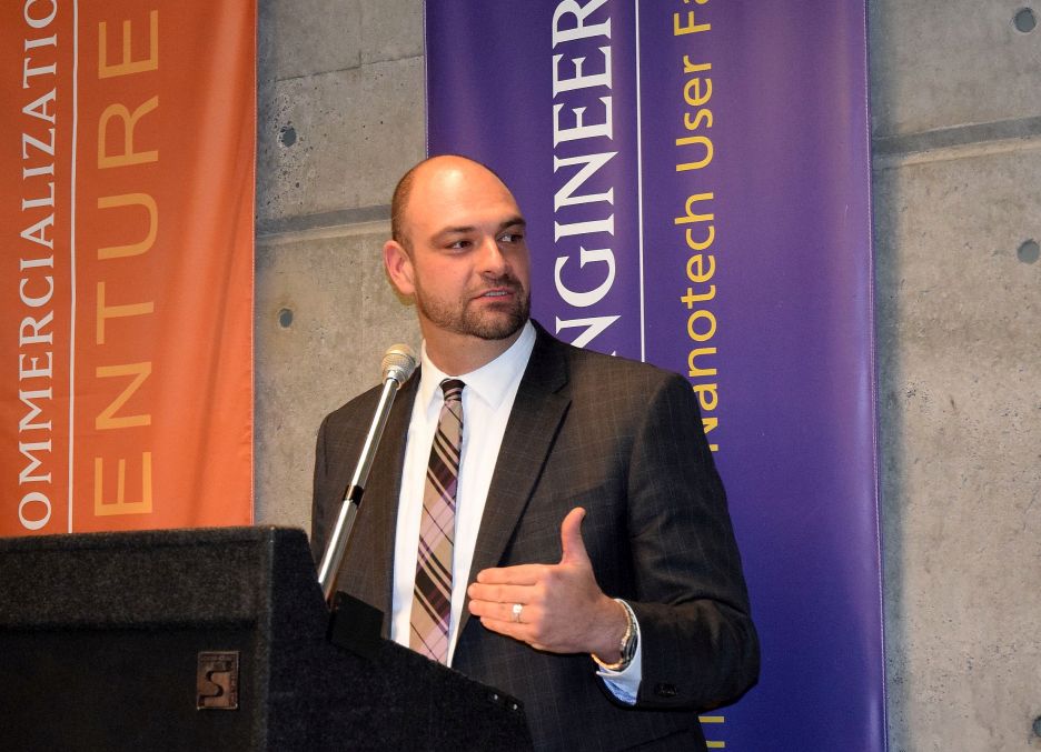
Michael Khbeis speaks at the ribbon-cutting ceremony celebrating the newly renovated Washington Nanofabrication Facility.
Prior to UW, Khbeis’ research was on enabling technologies for 2.5D/3D integration and flexible electronic systems for the Department of Defense. Exemplar technological developments include novel low profile packaging, plasma activated covalent bonding, and high aspect ratio sub-micron through silicon vias for high density interconnect and patents for stacked systems thermal management. In order to develop these capabilities, he managed, designed and oversaw construction or renovation of three cleanroom laboratories and specified, acquired, installed and commissioned over 40 major semiconductor fabrication and advanced packaging tools. As a technology mission leader, serving as research and engineering division chief (2009-2011) and branch chief (2005-2009), he was one of the youngest researchers to achieve executive grade in his agency. Khbeis obtained his Ph.D. in electrical engineering in 2010 (University of Maryland), MSEE in 2007 (University of Maryland) and BSEE in 2001 (UW). His academic research was focused on ambient vibration energy scavenging using microelectromechanical systems (MEMS). While an undergraduate, Khbeis also worked full-time as a semiconductor process and HAZMAT technician for Matsushita Semiconductor Corp of America (MASCA aka Panasonic) — 2017 marks his twentieth year in the semiconductor industry.